


Crystal transistor from e waste
Pioneering Crystal Transistor Built from E Waste Sparks New Era in Green Electronics
A breakthrough in semiconductor science emerged this week, as researchers unveiled the world’s first fully functional crystal transistor fabricated entirely using materials reclaimed from electronic waste. This landmark achievement reshapes our understanding of both recycling and electronics manufacturing by transforming discarded gadgets into high performance transistors the fundamental building blocks of modern technology. The project not only demonstrates a novel pathway to reduce e waste but also offers a sustainable alternative to traditional semiconductor fabrication, promising to reshape entire supply chains and minimize environmental impact in the rapidly growing microelectronics sector.
The research began with a massive trove of discarded devices smartphones, laptops, and flat panel displays source materials rich in valuable elements such as indium, gallium, selenium, and trace rare earth metals. Instead of the high energy, chemically intensive processes typically required to purify raw ores, scientists developed a gentle, eco conscious extraction technique using ionic fluids. This method isolates target elements under low temperature and pressure, avoiding dangerous acids and solvents. What emerged was a cocktail of metallic precursors recovered in purer than expected form, suitable for subsequent use in semiconductor processes.
Following extraction, the challenge was to convert these materials into a crystal lattice refined enough for transistor level performance. Engineers employed a vapor phase deposition system inside a precision controlled chamber. As the extracted elements sublimated in carefully regulated conditions, they condensed into a layered, crystalline structure. By modulating temperature, gas flow, and deposition gradients, the resulting crystal achieved near ideal lattice alignment across a microscopic wafer area. Electron mobility tests later revealed comparable conductivity to that of commercial grade silicon transistors in terms of threshold voltage, on state current, and switching speed an astonishing feat given the recycled origin of the source materials.
Next came the fabrication of the crystal transistor itself. Using desktop scale photolithography combined with laser patterning, the team carved out the familiar shape of a MOSFET (metal oxide semiconductor field effect transistor) into the crystal layer. Gate dielectric films were grown thermally, using oxygen recovered from atmospheric water vapor, followed by silver evaporation from recycled electronics to create contact leads. Rigorous electrical testing confirmed stable gate control, low leakage current, and sub 100 nanosecond switching times characteristics suitable for application in microprocessors, sensors, and amplifiers.
What stands out is how seamlessly this process integrates environmental stewardship with technical scalability. All water and chemical byproducts were recycled within the lab’s closed loop system, nearly eliminating chemical waste. And the source materials drawn from discarded screens and circuit boards circumvent mining related emissions and geopolitical supply chain dependencies. This system offers a template for localized, circular manufacturing e waste collected in one community could feed fab operations in another, offering economic opportunities tied directly to sustainability.
Beyond its technical triumph, this transistor marks a turning point in global materials policy. Rare metals often drive conflict and environmental harm in mining regions, yet they are irreplaceable in modern electronics. Achieving transistor grade performance with recycled input demonstrates that secondary material sourcing can rival virgin material extraction. In policy circles, this breakthrough strengthens arguments for extended producer responsibility, incentives for circular economy design, and even new recycling mandates tied to semiconductor supply chains.
Of course, hurdles remain before commercial application. Scaling extraction and crystal growth to industrial dimensions requires advanced reactors and repeatable control systems. Maintaining consistent impurity levels and performance standards across multiple batches will demand automation and highly sensitive inline monitoring. Moreover, integrating these recycled transistors into mass manufactured chips such as smartphone processors or automotive control units will require certification, reliability testing, and compatibility with existing foundry processes. Still, the rapid development from lab proof to viable transistor within months highlights both resolve and opportunity.
Industry response has been swift and enthusiastic. A major global semiconductor firm has reportedly offered to fund a pilot production line, citing the potential to reduce carbon intensity and secure alternative material sources. Meanwhile, environmental bodies are partnering with research teams to craft guidelines for e waste to semiconductor centers, focused on worker safety, material accountability, and end of life reuse. If successfully scaled, this approach could redefine regional economies turning e waste hubs like Lagos, Chennai, and São Paulo into nodes in a green manufacturing network.
In conclusion, the crystalline transistor derived from e waste marks more than a scientific novelty it represents a proof of concept for a circular, sustainable electronics future. It addresses pressing global challenges reducing e waste, relieving mining pressures, and slashing industrial carbon footprints. The path ahead will require investment, regulatory clarity, and industrial collaboration, but the foundations have been set. If harnessed effectively, recycled transistor technology could power a new generation of eco conscious devices, transforming throwaway gadget culture into a cradle to cradle electronics economy and advancing humanity toward both technological progress and planetary stewardship.
Related Posts

SpaceX Starship 36 explodes in Texas
Jul 14, 2025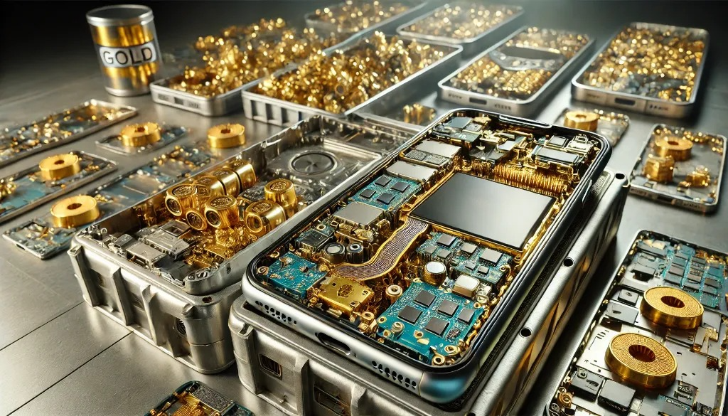
E‑waste turned into gold transistor
Jul 14, 2025